|
Power LED
Strobe
for PIC12F629 / 675
|
 |
Description
|
This project functions as a
simple strobe for driving a high power type LED. The output
driver provides current limiting suitable for use with either
350mA / 1 Watt LEDs or 700mA / 3 Watt LEDs.
Output from these LEDs is
extremely bright and visible from a considerable distance, even
in daylight.
Four jumpers provide options
for changing the pulse width, strobe repeat interval and single or double
strobe flash. There is also a Strobe Inhibit input that
can be used to stop the strobe pulse using a switch. The programmer ready code has default
timings which are easily customised by editing values in the PIC's EEPROM at programming time. |
|
 |
Warning.
The light output from Power LEDs is very intense. Avoid
looking directly at the LED when operating. |
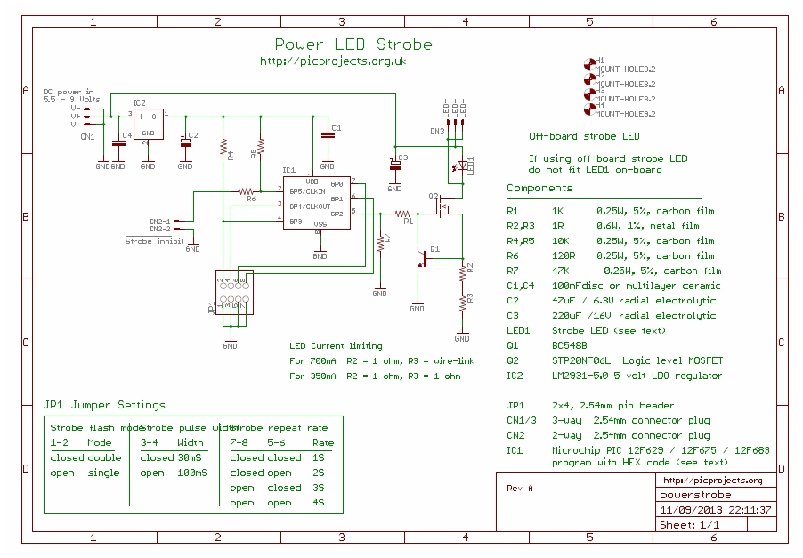
Schematic
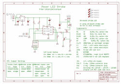  
Download
schematic in PDF

Circuit Description
The circuit provides a LED
strobe function with jumper selectable operating modes.
Firmware running in the PIC microcontroller produces precise
control of the strobe output pulse while an inhibit input allows
an external signal or switch to inhibit operation.
The strobe interval can be
configured using 4 jumpers for 1,2,3 or 4 seconds; strobe on time of 30mS or
100mS and single or double strobe pulse. Timings are
stored in the PICs EERPOM and can be customised as needed.
High power LEDs ideally need
driving with a current source to maintain a constant fixed current through the
LED. In this application I've used a simple linear current
limiter around Q1 and Q2. Since the LED is driven with
very short pulses and relatively long intervals between them the
average power dissipation is very low and neither the LED
or the output MOSFET require heatsinks.
Resistors R2+R3 set the current
limit. With R2 = 1 ohm and a wire link for R3, current is
set to 700mA. Using a 1 ohm resistor for both R2 and R3
(for a total of 2 ohms) sets the limit to 350mA.
LED1 connects between the
positive supply and the drain of
logic-level MOSFET Q2. The source of Q2 connects to
ground via R2+R3. When Q2 turns on the current passing
through the resistors R2+R3 causes a voltage drop to appear
across them. (Ohms law V= I x R ). The base of Q1 is
connected across the resistors and when the voltage reaches
about 0.7 volts, Q1 begins to turn on. The
collector of Q1 is connected to the gate of Q2 so so as it turns
on it pulls the voltage on the gate of Q2 towards ground, which
starts to turn Q2 off. This settles at a point where a
constant current is passed through R2/R3.
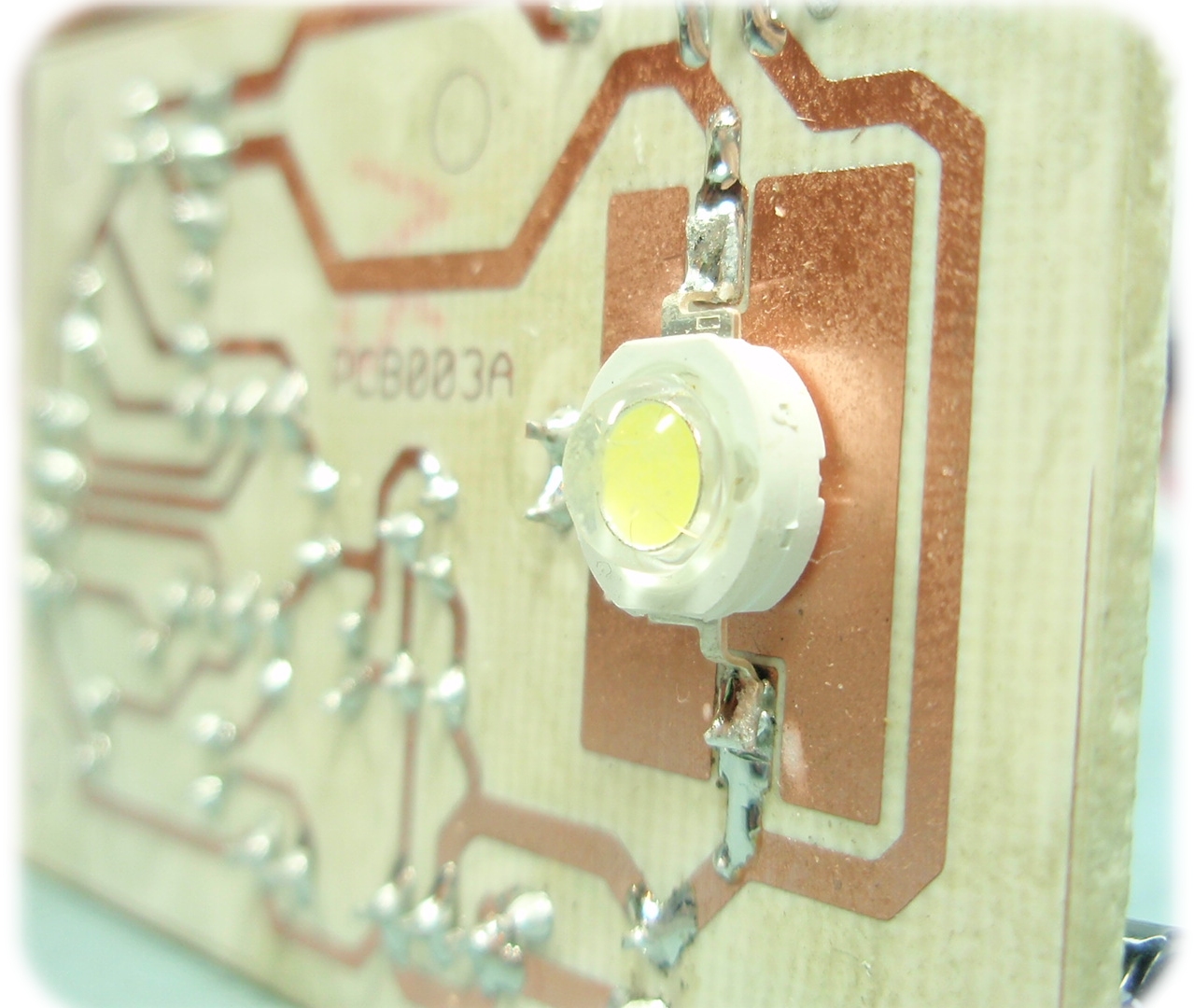
The strobe LED can either be
installed on the PCB in position LED1 or off-board via connector
CN3. If the off-board option is used do not install a LED
into position LED1 on the PCB.
Capacitor C1 is used to
decouple the 5 volt power supply rail. If you are building the
circuit on a breadboard or stripboard you should ensure it is
located close to the PICs Vdd connection (pin 1).
Capacitor C2 and C4 are
required by the LDO voltage regulator to stabilise its output.
The original design uses an LM2931-5.0 LDO regulator designed
for automotive applications. It can withstand reverse
polarity connection and 60 volt spikes at the input. You
can substitute other LDO regulators or a 78L05. If you use
a 78L05, minimum input voltage needs to be 7.5 volts.
The input voltage should be
between 5.5 and 9 volts smoothed DC. The power supply
needs to be able to supply in excess of 700mA, so a supply rated
at 1 amp or greater is ideal. You can use batteries to
power the circuit but they will need to be able to supply the
high currents required by the LED. The 7.2 volt
rechargeable battery packs used with RC models would be ideal
for this.
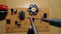
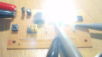
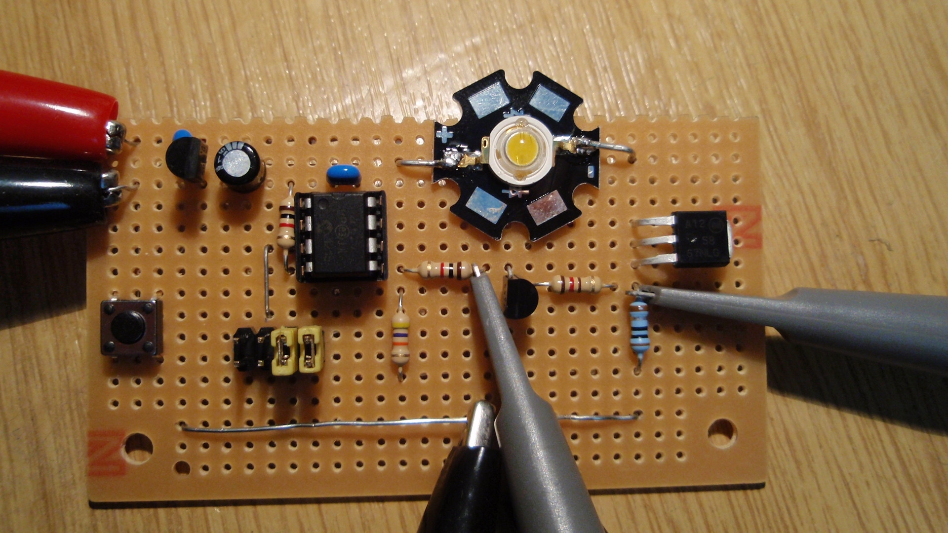
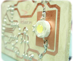
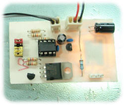
photos above show
development of the power LED strobe
Strobe inhibit control
The GPIO5 input to the PIC
functions as a Strobe Inhibit. When the input is held low,
the strobe output is inhibited. If you don't need this
feature, you can omit resistors R5 and R6 and leave the pin
disconnected as it has internal weak-pull enabled.
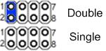
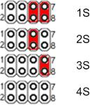
Mode Jumpers
The Strobe operating modes are
selected by using jumper block JP1. If you are building
the strobe for a specific application you may want to hardwire
inputs to ground as required rather than fit the jumper pin
header.
LED1 Options
The design will work with
either 350mA or 700mA LEDs. If a 350mA LED is used,
populate R2/R3 with 1 ohm, 0.25 watt, 1% resistors. If a
700mA LED is used, substitute a wire-link for one of the
resistors and use a single 1 ohm, 0.6 watt 1% resistor for the
other.
We avoid the need for heatsinks
on the LED and output MOSFET by using a very short duty cycle.
It is important not to allow the LED to remain on continuously
either through a fault or by modifying the pulse
width/repetition rate
You can drive up to three LEDs
in series using CN3 to make the external connection. The
power supply input voltage needs to be greater than the sum of
the forward voltages of the LEDs + 1 volts
For example: If you are
using two white LEDs with a forward voltage of 3.6 volts, the
power supply input voltage should be: 2 x 3.6 volts + 1 volt =
8.2 volts. In this case a 9 volt power supply would be
ideal. For three LEDs in series use a 12 volt power
supply.
MOSFET Types
This circuit is designed around
a logic-level MOSFET for Q2 which has a gate threshold voltage
of around 2.5 volts. You may find standard, non logic
level MOSFETs with higher gate threshold voltages can't turn on
sufficiently to provide 700mA of current to the LED.
Although the LED will be on and may appear very bright, it won't
be operating at the desired 700mA current.
I've tested this circuit with
STP36NF06L, STP20NF06L and NTD5867NL. The NTD5867NL
comes in IPAK-369D through-hole and DPAK smd package types so
doesn't fit the PCB layout but is ideal if you want to do your
own compact design.
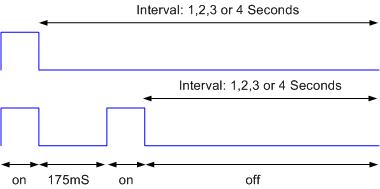
Strobe Operating Modes
This section refers to the
default timings used in the programmer ready firmware download.
The pulse width, interval and
strobe mode are user selectable using the JP1 jumper block.
There are two strobe modes, single and double pulse. The
double mode has a (default) 175mS off-time between the two pulses.
As shown in the diagram below, the interval is measured from the
end of one pulse group to the start of the next group.
Default timing
Jumper Settings
 |
Strobe
Mode
JP1 (1-2)
|
Pulse
Width
JP1 (3-4)
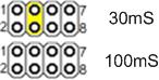
|
Interval
JP1 (5-6,7-8)
|
Customising the strobe
timing
The timers for the pulse width,
interval and double mode gap are all configurable by editing the
values in the PICs EEPROM before writing the HEX into the PIC.
This is nice and easy to do and doesn't require reassembling the
code or anything complicated. Just load the HEX file from
the firmware download section into your programmer application.
Edit the values in the EEPROM as shown below and then write the
code and EEPROM data into the PIC.
Suppose you want a pulse width
of 40mS (40 x 1mS) and an interval of 1.3 Seconds (13 x 100mS) you would
set
the data in address 00 to 28 (40 decimal == 28
hexadecimal). For the 1.3 second interval change the data
in address 03 to 0D (13 decimal == 0D hexadecimal).
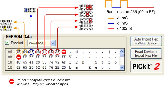
Values shown in the example
above are the default values in the firmware download. If
you don't modify them it will uses these timings.
Converting decimal values to
hexadecimal
Depending on your programmer
the values you need to enter will probably be in hexadecimal, easiest way to
convert decimal values to hexadecimal is Google, see example
below. The prefix 0x in the result simply tells us the
value is in hexadecimal (hex for short).

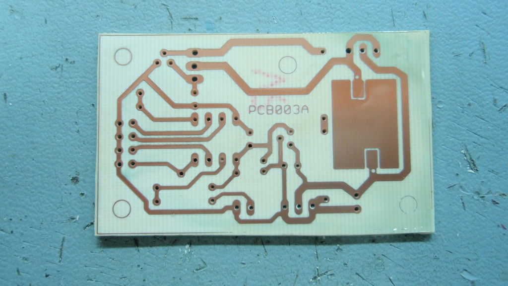
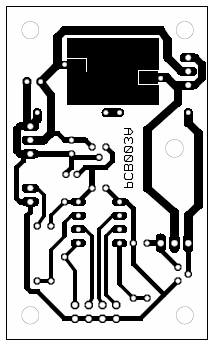
PCB Layout
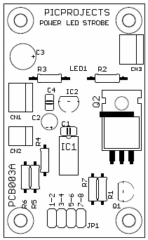
Download PCB
artwork in PDF
Download PCB
overlay in PDF
Component List
You can buy all the parts
needed to build this project from most component suppliers world
wide. In the UK you can get everything from Rapid Online and
I've included a parts list with their part numbers below.

All
Rapid parts/descriptions correct at 11 September 2013. You should
check part# and descriptions are correct when ordering in case
I've made a mistake transferring them onto this page.
|
Component |
Description |
Part # |
| R1 |
1k Cr25 0.25w Cf
Resistor - Pack of 100 |
62-0370
|
| R2,R3
* |
1r 1% 1w Metal Film
Resistor (each) |
62-7890 |
| R4,R5
|
10k Cr25 0.25w Cf
Resistor - Pack of 100 |
62-0394
|
| R6 |
120r Cr25 0.25w Cf
Resistor - Pack of 100 |
62-0348 |
| R7 |
47k Cr25 0.25w Cf
Resistor - Pack of 100 |
62-0410 |
| C1,C4 |
100nf 2.5mm Y5v
Dielect Ceramic Capacitor |
08-0270 |
| C2 |
47uf 16v Radial
Electrolytic Capacitor |
11-3726 |
| C3 |
220uf 16v Radial
Electrolytic Capacitor |
11-3702 |
| Q1 |
BC548B TRANSISTOR TO92
30V NPN (RC) |
81-0066 |
| Q2
** |
Stp36nf06l Mosfet
Logic N 60v 30a |
47-0552 |
| IC1
** |
PIC12F629-I/P (RC) |
73-3262 |
| IC2
* |
Lp2950cz-5 Micropower
Regulator. |
82-0680 |
| LED1 |
w 3.3v White Power LED
200lm |
55-2003 |
| socket for IC1 |
8 Pin 0.3in Turned Pin
Socket |
22-1720 |
| JP1 |
4+4 WAY DOUBLE ROW
HEADER PLUG RC |
22-0555
|
| CN1, CN3 |
3 Way
2.54mm KK Molex Straight Header |
22-0840 |
| CN2 |
2 Way
2.54mm KK Molex Straight Header) |
22-0838 |
| order 4
|
OPEN BLUE 2.54MM
JUMPER LINK (RC) |
22-3555
|
| |
|
|
Parts List Notes
*
Rapidonline don't supply some
parts I used so I've specified alternative parts which should
work.
**
Alternate MOSFETs are STP20NF06L,
NTD5867NL
***
The PIC12F629 will need
programming with the firmware at the bottom of this page.
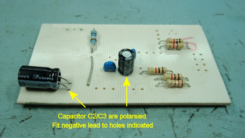
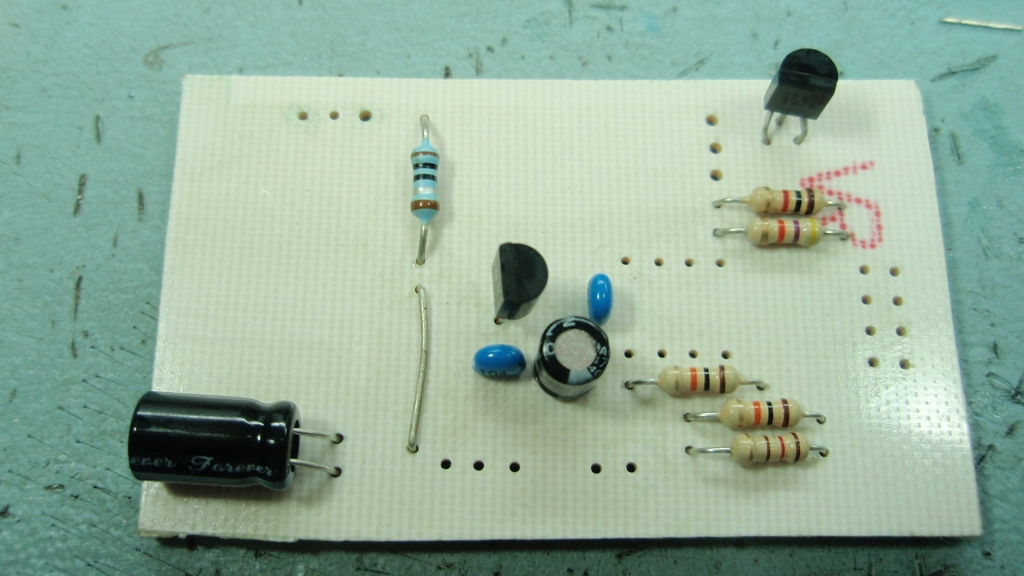
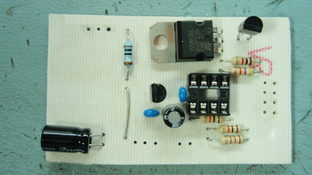
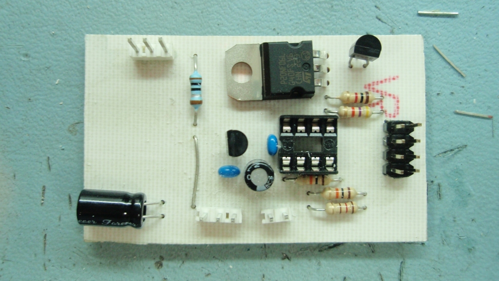
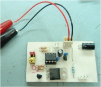
Construction photos:
Construction is very
straightforward. Fit the components in the order shown in
photos Fig 1 to Fig 6.
Fig 3. The two
electrolytic capacitors must be installed the correct way round.
The negative terminal is normally the shorter lead, it is also
marked on the side of part.
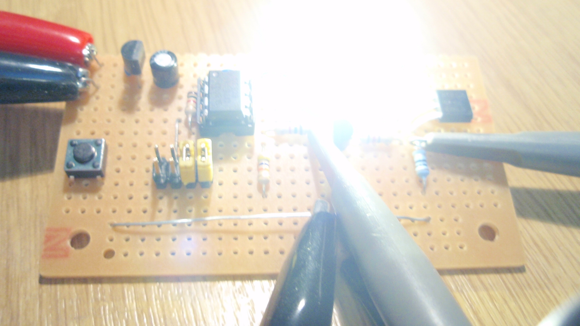
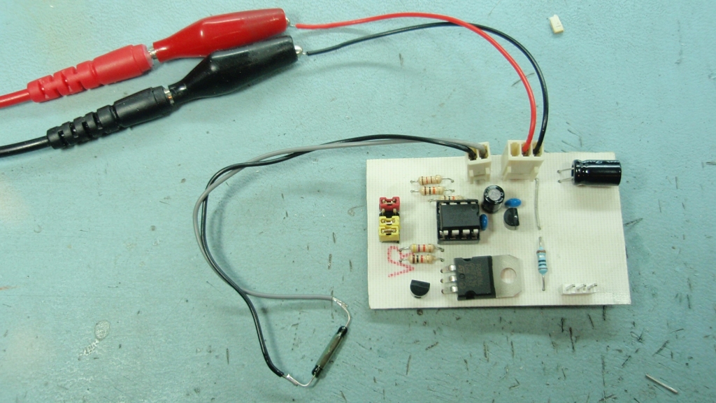
Fig 6. When you get the board assembled up to figure 6, connect
power to the board and check the voltage between pins 1 and 8 of
the IC1 socket. It should measure 4.9 to 5.1 volts, if it
doesn't don't continue until you have found out why and
rectified the fault.
Pin header C2 is only used if
you want to connect an external inhibit switch.
Pin header C3 is only used if
you want to connect an external LED. If you are using an
external LED, don't connect the on-board LED as well. It's
either on-board or external, not both.
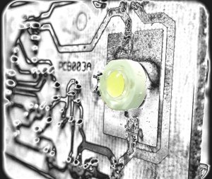
Fig 7. The power LED is
soldered to the copper side of the PCB. Make sure to
connect the anode and cathode terminals the correct way round.
Fig 8.
 Avoid looking
directly at the LED when testing and operating the board.
The intense light output may damage your eyes. Avoid looking
directly at the LED when testing and operating the board.
The intense light output may damage your eyes.
Fig 9. Fully assembled
board with power connected to CN1 and a magnetic reed switch
connected to CN2 strobe inhibit input.

Fig.1 |
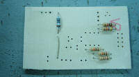
Fig .2 |
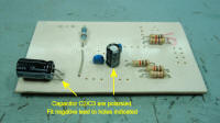
Fig. 3 |
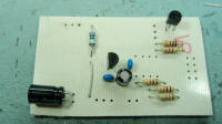
Fig.4 |

Fig.5 |

Fig.6 |
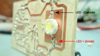
Fig.7 |
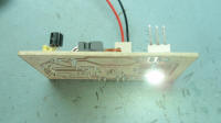
Fig.8 |

Fig.9 |
Power Supply
The LED Strobe circuit ideally
needs a DC power supply in the range 5.5 to 9 volts and rated
for 1 amp or more. With the LDO regulator specified you could use 4 x 1.5V AA
high capacity Alkaline batteries (Not NiMH rechargeable as 4.8
volts output is insufficient to operate correctly)
If you want to use rechargeable batteries the 7.2 volt battery
packs used with Radio Controlled models would be ideal.
Firmware
You can use either a PIC 12F629
or 12F675 microcontroller with this circuit. The same
firmware code is used with either device. Download
the files required below.
The HEX file is ready to
program straight into the PIC. The asm file is the
source code which you can modify or just view to see how it
works.
Not got a programmer? Buy
a pre-programmed PIC from the
On-line store
|
Description |
Filename |
Download link |
| Source
code for 12F629/675 |
ledstrobe-PWR.asm |
 download
 |
HEX file
ready to program into the PIC
for use with 12F629 & 12F675 |
ledstrobe-PWR.HEX V1.0.0 09/09/2013 |
download |
If you need a PIC Programmer I
strongly recommend the
Microchip PICKit 2,
this is available from suppliers world wide or direct from
Microchip. It's reasonably cheap to buy and reliable.
Troubleshooting
If the LED outputs blink 3 or 4
times at regular intervals and the jumper settings are
ineffective this indicates one of two fault conditions.

- The EEPROM data at addresses 07
and 08 must be 0xA9 and 0x56 respectively. If this is not
correct the 3 blink error code will be shown. You can
correct the error by reprogramming the EEPROM ensuring these
validation bytes are correct.
- If the OSCCAL calibration word is
missing the 4 blink error code will be shown. You will
need to recalibrate the PIC using a PICkit2 programmer, or the
recalibration project here
Contact us:
 |