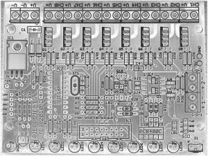
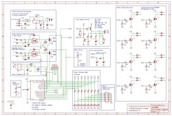
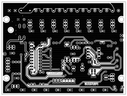
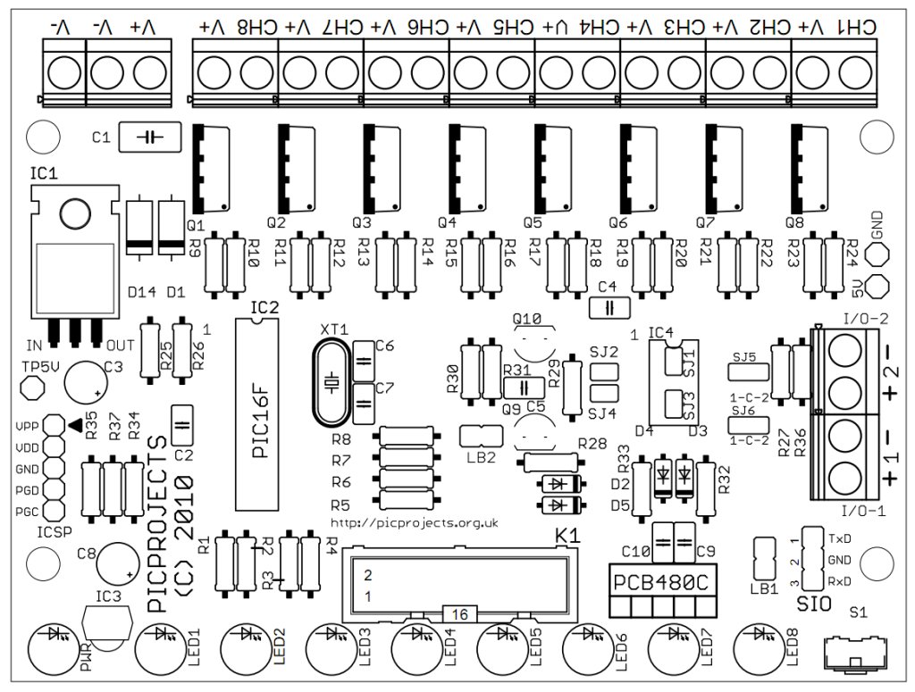
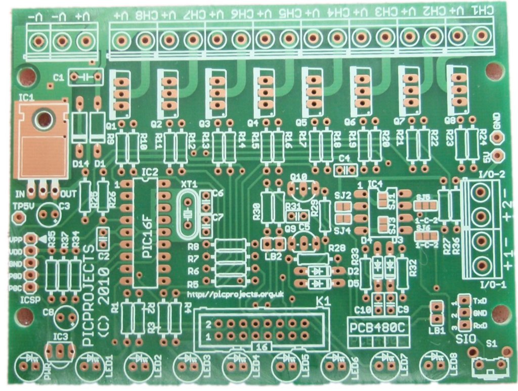
As the schematic shows the
board contains a number of sub-circuits which can be included or
omitted as required.
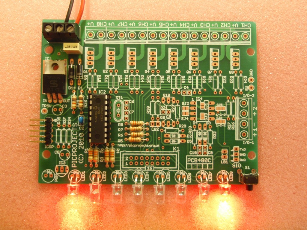
The power supply section uses a
7805 positive 5 volt regulator, the provision of C3 enables the
use of an LDO regulator such as the LM2940CT-5 which requires a
large (47µF) for stability. Diode D1 provides reverse
polarity protection and D14 protects against reverse biasing of
the regulator output should the board be connected to an
external 5 volt supply.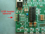
The board is designed for the
18 pin Microchip PIC16F devices including 16F84A, 16F627A,
16F628A, 16F648A, 16F88* and the new Enhanced midrange parts
16F1826 / 16F1827. The provision for an external crystal
and load capacitors allows designs to use higher clock speeds or
more accurate timing over the internal RC oscillator module.
A 5 pin ICSP connection is also made available for in-circuit
programming and debugging.
* The 16F88 uses different
I/O pins for the ASUART so it can't use the serial hardware
interface on the PCB
An Infra Red Receiver module
such as the TSOP4838 can be used with the board, the output
connecting to RB0 I/O pin.
Switch S1 provides user input
and connects to RA4 with provision for a 10K pull-up resistor.
The lower four I/O pins of Port
A and the high four I/O pins of PORTB are connected via
resistors to on-board LEDs and also to a 16 pin header.
The header allows 8 I/O lines to be used externally via an IDC
cable connection. These same eight I/O outputs can also
connect to STP36NF06 or STP20NF06L logic-level N-Channel MOSFETs for driving
high power loads. The MOSFET drains are connected to
5.08mm 16 amp terminal block connections. Each channel can
handle 3 amps, however the combined channel current for the
whole board should not exceed 16 amps.
A discrete RS232 level shifter
is included allowing the board to connect to external equipment
using serial comms. Since this circuit doesn't have a -12
volt supply it makes use of the RxD input from the host
equipment to 'steal' the negative supply for the boards TxD
output. Generally this works well but does rely on the
host comms equipment using RS232 signal levels. The input
for the SIO is a 3-pin 2.54mm header. The centre pin is
ground and the outer pins are Rxd/Txd. This arrangement
allows rotation of the connecting socket through 1800
to convert input connection from DTE to DCE.
n.b. The 16F88 uses different I/O pins for the RX/TX AUSART
peripheral to those used by the 16F627A/8A and 16F1826/7 devices
so the serial hardware cannot be used with this part.
The final option is the
provision of two external input/output connections. The
input mode can either use the opto-isolator or by omitting the
opto-isolator and shorting the solder jumpers on the PCB provide
direct access to I/O pins for use with digital or analogue
inputs.
The opto-isolator does not
provide high voltage isolation since the signals are routed in
close proximity to other signals on the main PCB. The main
reason behind its inclusion is to provide ground isolation and
input protection.
When the Opto-isolator IC is
not used the I/O-1/2 connectors provide direct connection to the
PICs I/O pins for use as either digital I/O or analogue inputs.
The resistor/diode/capacitor on each connection allows input
filtering or output slew rate control. Pull-up resistors
are also provided on these inputs. These components can be
included/omitted, values altered etc. to suit whatever
application the I/O pin is used for.
The SJ1 and SJ2 solder jumpers
will also take an 0805 SMD resistor allowing a resistor to be
inserted between the PIC I/O pin and capacitors C9/C10.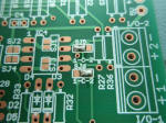
Solder jumpers SJ5 and SJ6
allow the two inputs to be routed to different I/O pins
SJ5 connects I/O-1 connector to
either RB1 (shared with the Serial I/O RXD input) or RB0 (shared
with the IR Receiver module)
SJ6 connects I/O-2 connector to
either RA4 (shared with switch S1 input) or RB3.
At the right hand edge of the
PCB next to the two I/O terminal blocks are solder points for
access to 5V and Gnd for external use.
Finally, a resistor and LED
across the 5 volt supply can be fitted for power-on indication.